Skip to main content
make a gift
About
Leadership & Staff
Researchers
Get Involved
Contact Us
Logo & Acknowledgments
Research
Solar Energy
Energy Storage
Energy Systems
Advanced Materials & Measurements
Find a Researcher
Affiliated Research Centers
Collaborative Seed Grants
Postdoctoral Research
Facilities
Washington Clean Energy Testbeds
Campus Research Facilities
Education
UW Graduate Students
Undergraduate Students
K-14 Engagement
Community Engagement
Community Research & Project Support
K-14 Engagement
Community-Led Events
News
Newsletter
Events
CEI Seminars
Special Events
Orcas Conference
Archive
2023-24 Graduate Fellows
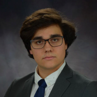
Jack Barlow
...
by
corinsr
September 21, 2023
2022-23 Graduate Fellows
Jiayi Zhu
...
by
corinsr
September 30, 2022
2022-23 Graduate Fellows
Chun-Chih Tseng
...
by
corinsr
September 30, 2022
2022-23 Graduate Fellows
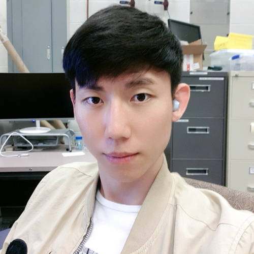
Heonjoon Park
...
by
corinsr
September 30, 2022
2022-23 Graduate Fellows
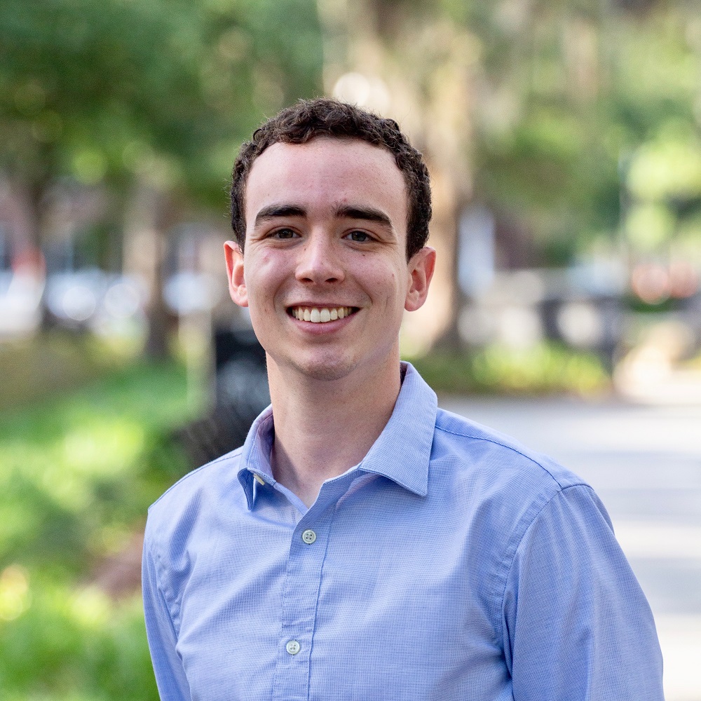
Eric Lester
...
by
corinsr
September 30, 2022
2022-23 Graduate Fellows
Jonathan DeStefano
...
by
corinsr
September 30, 2022
2022-23 Graduate Fellows
Jared Abramson
...
by
corinsr
September 30, 2022
2021-22 Graduate Fellows
Tharindu W. Fernando
...
by
corinsr
October 6, 2021
2021-22 Graduate Fellows
John Cenker
...
by
corinsr
October 5, 2021
2020-21 Graduate Fellows
Graduate Fellows
Christian Pederson
...
by
corinsr
October 19, 2020
2020-21 Graduate Fellows
Jiaqi Cai
...
by
corinsr
September 17, 2020
2020-21 Graduate Fellows
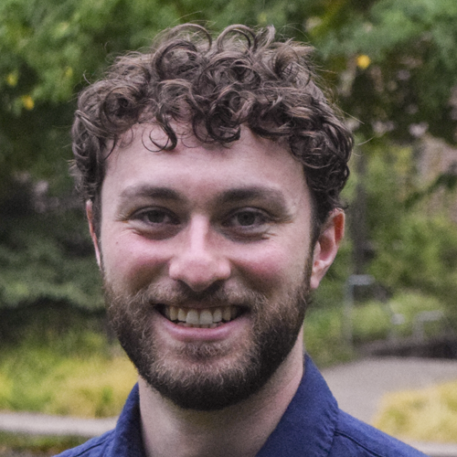
Kyle Hwangbo
...
by
corinsr
September 2, 2020
1
2
3
4
5
« Previous Page
Next Page »